
한국 정부가 오는 2047년까지 세계 최대 반도체 메가 클러스터 구축에 총력을 기울인다. The country will build by 2047 the world’s largest semiconductor cluster in Gyeonggi-do Province.
산업통상자원부와 과학기술정보통신부는 15일 윤석열 대통령이 경기 수원 성균관대학교 반도체관에서 주재한 ‘국민과 함께하는 민생 토론회’에서 ‘세계 최대·최고 규모의 반도체 메가 클러스터 조성 방안’을 발표했다.
The Ministry of Trade, Industry and Energy and the Ministry of Science and ICT on Jan. 15 released their plan for this at a policy debate under the theme “Semiconductor Industry for Enriching Public Livelihood.” President Yoon Suk Yeol chaired the event held at the Natural Sciences Campus of Sungkyunkwan University in Suwon, Gyeonggi-do.
반도체 메가 클러스터는 경기 평택, 화성, 용인, 이천, 안성, 성남, 판교, 수원 등에 밀집한 반도체 기업과 기관을 한데 아우르는 개념이다.
The envisioned mega-cluster will cover cities in the province packed with semiconductor companies and institutions: Pyeongtaek, Hwaseong, Yongin, Icheon, Anseong, Seongnam and its district of Pangyo New Town, and Suwon.
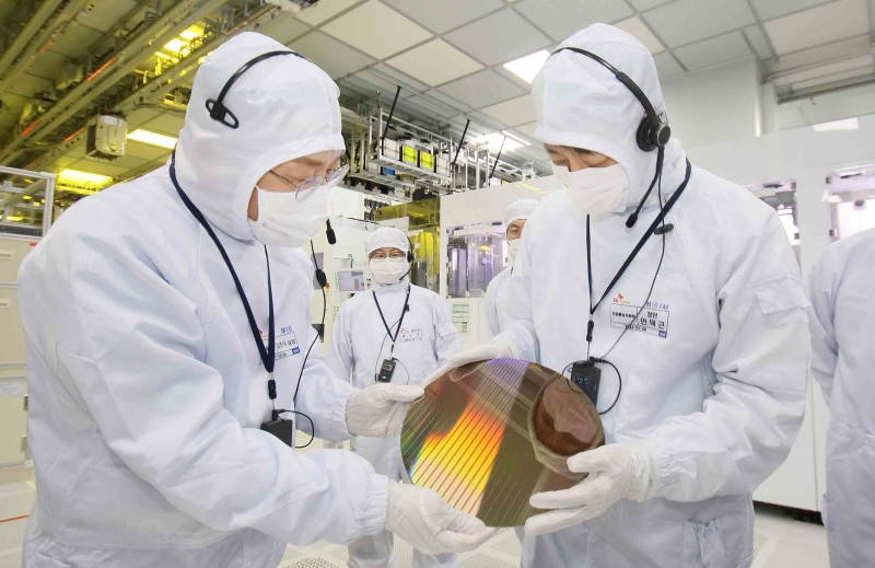
발표에 따르면 현재 19개의 생산팹과 2개의 연구팹이 집적된 메가 클러스터에 2047년까지 삼성전자와 SK하이닉스 등 총 622조 원의 민간 투자를 통해 16개(생산팹 13개, 연구팹 3개)의 신규팹이 신설된다. 2027년까지 생산팹 3기, 연구팹 2기가 먼저 완공될 전망이다.
The report said the facility in 2047 will have 13 production and three R&D fabs added to its existing lineup of 19 production and two R&D fabs through private investment from Samsung Electronics and SK Hynix worth a combined KRW 622 trillion. The first three production and two R&D fabs are set for completion first by 2027.
특히 여의도 7배에 해당하는 2100만m² 부지에서 2030년 기준 월 770만장의 웨이퍼를 생산해 세계 최대 생산량을 달성한다는 계획이다.
Another goal is to have the world’s largest monthly output of 7.7 million wafers by 2030 at a production site spanning a massive 21 square km.
정부는 이번 메가 클러스터 조성으로 소부장 및 팹리스 등 협력기업 생태계의 동반 성장과 함께 650조 원의 생산 유발효과, 346만개의 직·간접 일자리 창출로 이어질 것이라고 내다봤다.
Construction of the cluster’s facilities, the government said, will lead to the joint growth of the related ecosystem such as for makers of materials, parts and equipment, and fabless companies. The expected results are a production-generating effect of KRW 650 trillion and the direct and indirect creation of 3.46 million jobs.
반도체 생산을 위한 인프라·투자환경 조성을 위해 정부는 전력·용수 등의 공급에 차질이 없도록 지원하고 인프라 설치 관련 인허가가 신속히 처리될 수 있도록 인허가 타임아웃제 등 이미 도입된 신속처리 제도를 적극 활용한다.
To create the proper environment for infrastructure and investment in chip production, public support will also ensure no disruptions to electrical power and water supply and the active use of expedited processing systems in use like a permit timeout policy for rapid processing of infrastructure-related permits.
반도체 예산도 전년 대비 2배 규모인 1조 3000억 원으로 편성하고 국무총리 주재 ‘국가첨단전략산업위원회’를 통해 반도체 킬러규제를 철폐해 나갈 예정이다.
The semiconductor budget of KRW 1.3 trillion is double that of the previous year and “killer regulations” for semiconductors will be lifted through the National High-Tech Strategic Industries Committee chaired by the prime minister.
이와 함께 정부는 해외 인재 유치를 위해 현재 1년인 사이언스 카드 비자 기간을 최대 10년으로 연장하고 제도 개선을 통해 해외 연구자의 국내 유입을 촉진한다. 국내 연구자의 해외 연구기관 파견도 추진해 첨단 기술 및 인력 교류를 활성화한다.
The science card visa will be improved and extended from one year to a maximum of 10 to attract global talent. Stimulation of the exchange of cutting-edge technology and personnel will allow the dispatch of domestic researchers to R&D institutes abroad.
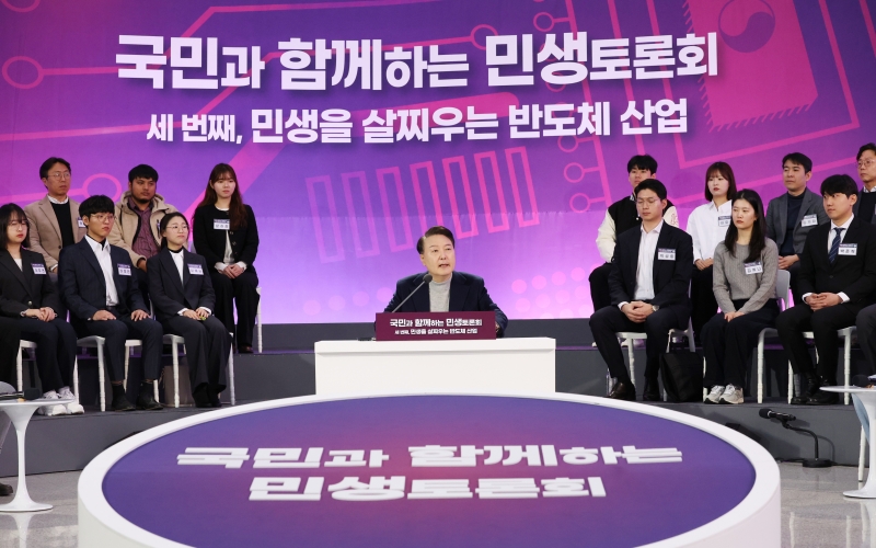
한편, 이날 토론회에서 윤 대통령은 모두 발언을 통해 “반도체는 그 어떤 산업보다도 민생을 풍요롭게 하고 많은 양질의 일자리를 제공한다”며 “반도체 산업은 국가의 인적·물적 자원을 총력 투입해야 성공할 수 있는 전략 산업”이라고 강조했다.
President Yoon said at the debate, “Semiconductors enrich the people’s livelihoods more than any sector and create many quality jobs,” adding, “Chips are a strategic industry that succeeds only if the country invests all of its human and material resources into it.”
이어 올해 끝나는 반도체 투자 세액공제도 앞으로 계속 적용하고 동맹, 우방국과의 외교관계도 강화해 반도체 산업을 강력히 뒷받침하겠다는 의지를 밝혔다.
He added his intent to extend tax credits for semiconductors expiring this year and his strong support for the industry by reinforcing diplomatic ties with allies and friendly countries.
박혜리 기자 hrhr@korea.kr
By Park Hye Ri, hrhr@korea.kr