
한국 연구팀이 머리카락 굵기 5분의 1에 불과한 초박형 반도체 칩을 10층 이상 안정적으로 쌓아 올리는 기술을 개발했다. 고대역폭 메모리(HBM)보다 집적 밀도를 4배나 높인 획기적인 성과다.
A joint research team has developed a stable stacking method of over 10 layers of ultra-thin semiconductor chips, each a fifth the thickness of a human hair, that raises integration density to four times that of high-bandwidth memory (HBM).
포항공과대학교(포스텍)과 한국생산기술연구원 공동 연구팀은 칩을 옮기는 동시에 금속 접합까지 가능한 새로운 공정을 개발, 기존 고성능 메모리보다 약 4배 높은 집적 밀도를 구현하는 데 성공했다고 지난달 30일 밝혔다.
Researchers from Pohang University of Science and Technology (POSTECH) and the Korea Institute of Industrial Technology on June 30 said they developed a process of transferring semiconductor chips and simultaneously creating metallic interconnections, resulting in integration density 400% higher than conventional high-performance memory.
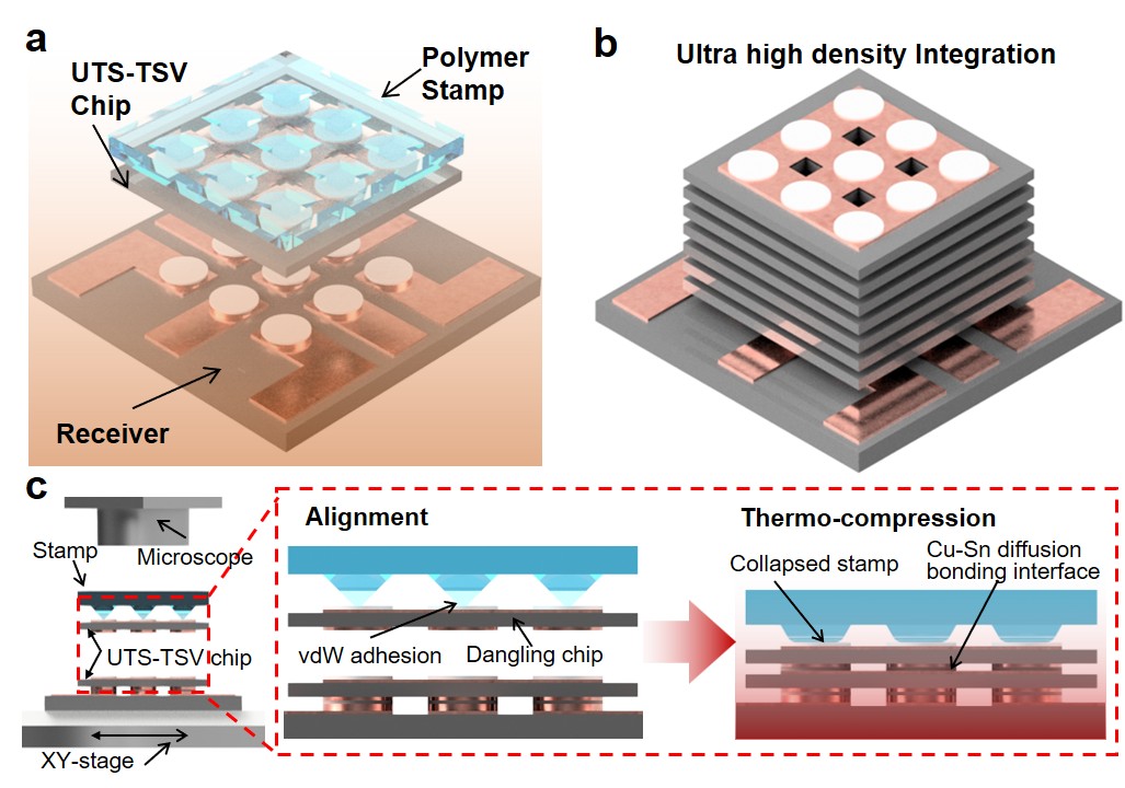
스마트폰은 갈수록 얇아지는 반면 반도체는 더 강력해져야 하는 상황에서, 반도체 업계는 칩을 옆으로 넓히는 대신 위로 높이 쌓는 구조에 집중하고 있다. 특히 AI 반도체의 성능을 좌우하는 HBM는 메모리 칩을 여러 개 층층이 쌓아 만드는 구조여서 얼마나 많은 칩을 안정적으로 쌓을 수 있는지가 핵심 경쟁력으로 꼽힌다.
As smartphones get thinner, semiconductors need to process enormous amounts of data at extremely high speeds. Thus the semiconductor sector is focusing on vertically instead of horizontally stacking chips.
HBM, which determines the performance of artificial intelligence semiconductors, is built by stacking multiple memory chips layer on layer, thus the technology to stack a high number of chips is considered a key competitive advantage.
문제는 칩이 얇아질수록 휘거나 깨지기 쉬워 다루기가 까다롭다는 점이다.
The problem is that a thinner chip is more susceptible to bending, warping and fracture, making it difficult to handle during manufacturing.
이에 연구팀은 칩을 원하는 위치에 정밀하게 옮겨 붙이는 ‘전사 프린팅’ 기술과 칩을 이송하는 순간 금속을 접합하는 ‘실시간 본딩’ 기술을 결합했다. 칩을 옮기고, 붙이고, 연결하는 세 가지 과정을 단 한 번의 공정으로 단축한 것이다.
To overcome this limitation, the team combined two technologies into a single process platform: transfer printing to precisely place chips in their intended positions and In-situ bonding to form metallic bonds simultaneously during chip transfer. This integrates chip transfer, placement and electrical interconnection into a single manufacturing step.
연구팀은 이 공정을 활용해 두께 약 14마이크로미터의 초박형 실리콘 칩을 180도 이하의 저온, 20킬로파스칼 이하의 저압 조건에서 칩을 10층 이상 안정적으로 쌓아 올리는데 성공했다. 쌓은 뒤에도 층간 정렬 오차가 작았고, 휨 현상도 최소화됐다는게 포스텍 설명이다. 같은 높이 안에 더 많은 칩을 담을 수 있는 길을 열게 된 셈이다.
Using the process, the team stably stacked over 10 ultra-thin silicon chips, each about 14 micrometers thick, at low temperatures below 180 degrees Celsius and low pressure below 20 kilopascals.
POSTECH said the stacked chips maintained high alignment accuracy with minimal warping, allowing the stacking of more chips within the same package height.
포스텍은 “이번 기술은 AI 반도체뿐 아니라 여러 기능의 칩을 하나의 패키지에 묶는 칩렛 기술, 초소형 발광소자를 활용한 마이크로 발광다이오드(LED) 디스플레이 분야에도 적용할 수 있다”며 “고성능 AI 반도체와 차세대 메모리 시스템 개발의 핵심 기반 기술로 활용될 것으로 기대한다”고 말했다.
“This technology is applicable not only to AI semiconductors but also chiplet-based technology, which integrates multiple functional chips into a single package, and micro-LED displays,” POSTECH said. “This is expected to emerge as a core foundational technology for developing high-performance AI semiconductors and next-generation memory systems.”
이번 연구 결과는 다학제 공학 분야 국제 학술지 ‘리절츠 인 엔지니어링(Results in Engineering)’ 온라인판에 게재됐다.
The study was published in the online edition of the international academic journal Results in Engineering.
샤를 오두앙 기자 caudouin@korea.kr
By Charles Audouin, caudouin@korea.kr